
On Optimization of Manufacturing of a Single Leg N-level Cascaded H-bridge Multilevel Inverters to Increase Integration Rate of Their Elements
Abstract
This paper presents an optimized manufacturing approach for a single-leg N-level cascaded H-bridge multilevel inverter, focusing on increasing the integration rate of its elements. By employing heterostructures composed of substrates and epitaxial layers, the proposed method incorporates doping techniques such as diffusion and ion implantation, followed by annealing processes to manage dopants and radiation defects. This strategy enables the reduction of element dimensions while maintaining high density and efficiency in integrated circuits. The paper further analyzes the dynamics of defect redistribution during annealing and introduces techniques to refine the manufacturing process for enhanced performance of bipolar heterotransistors.
Keywords:N-level cascaded H-bridge inverterIntegration rate optimizationBipolar heterotransistorsDoping
and annealing, Semiconductor manufacturing techniques.
1. Introduction
An actual and intensively solving problems of solid state electronics is increasing of integration rate of elements of integrated circuits (p-n-junctions, their systems et al) [1]–[8]. Increasing of the integration rate leads to necessity to decrease their dimensions. To decrease the dimensions are using several approaches. They are widely using laser and microwave types of annealing of infused dopants. These types of annealing are also widely using for annealing of radiation defects, generated during ion implantation [9]–[17]. Using the approaches gives a possibility to increase integration rate of elements of integrated circuits through inhomogeneity of technological parameters due to generating inhomogenous distribution of temperature. In this situation one can obtain decreasing dimensions of elements of integrated circuits [18] with account Arrhenius law [1], [3]. Another approach to manufacture elements of integrated circuits with smaller dimensions is doping of heterostructure by diffusion or ion implantation [1]–[3]. However in this case optimization of dopant and/or radiation defects is required [18].
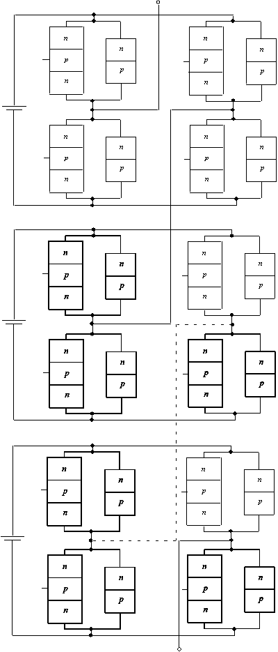
In this paper we consider a heterostructure. The heterostructure consist of a substrate and several epitaxial layers. Some sections have been manufactured in the epitaxial layers. Further we consider doping of these sections by diffusion or ion implantation. The doping gives a possibility to manufacture bipolar heterotransistors framework a single leg N-level cascaded H-bridge multilevel inverter so as it is shown on
2. Method of Solution
In this section we determine spatio-temporal distributions of concentrations of infused and implanted dopants. To determine these distributions we calculate appropriate solutions of the second Fick's law [1], [3], [18].
Boundary and initial conditions for the equations are
The function C(x,y,z,t) describes the spatio-temporal distribution of concentration of dopant; T is the temperature of annealing; DС is the dopant diffusion coefficient. Value of dopant diffusion coefficient could be changed with changing materials of heterostructure, with changing temperature of materials (including annealing), with changing concentrations of dopant and radiation defects. We approximate dependences of dopant diffusion coefficient on parameters by the following relation with account results in Refs [19]–[21].
. (3)
Here the function DL (x,y,z,T) describes the spatial (in heterostructure) and temperature (due to Arrhenius law) dependences of diffusion coefficient of dopant. The function P (x,y,z,T) describes the limit of solubility of dopant. Parameter [1,3] describes average quantity of charged defects interacted with atom of dopant [19]. The function V (x,y,z,t) describes the spatio-temporal distribution of concentration of radiation vacancies. Parameter V* describes the equilibrium distribution of concentration of vacancies. The considered concentrational dependence of dopant diffusion coefficient has been described in details in [19]. It should be noted, that using diffusion type of doping did not generation radiation defects. In this situation 1= 2= 0. We determine spatio-temporal distributions of concentrations of radiation defects by solving the following system of equations [20], [21].
Boundary and initial conditions for these equations are
Here =I,V. The function I (x,y,z,t) describes the spatio-temporal distribution of concentration of radiation interstitials; D(x,y,z,T) are the diffusion coefficients of point radiation defects; terms V2(x,y,z,t) and I2(x,y,z,t) correspond to generation divacancies and diinterstitials; kI,V(x,y,z,T) is the parameter of recombination of point radiation defects; kI,I(x,y,z,T) and kV,V(x,y,z,T) are the parameters of generation of simplest complexes of point radiation defects.
Further we determine distributions in space and time of concentrations of divacancies V(x,y,z,t) and diinterstitials I(x,y,z,t) by solving the following system of equations [20], [21].
( , , , ) ( , , , ) ( , , , ) = [ ( , , , ) ] + [ ( , , , ) ] +
( , , , ) + [ ( , , , ) ] + , ( , , , ) ( , , , ) − ( , , , ) ( , , , )
( , , , ) ( , , , ) ( , , , ) = [ ( , , , ) ] + [ ( , , , ) ] +
( , , , ) 2
+ [ ( , , , ) ] + , ( , , , ) ( , , , ) − ( , , , ) ( , , , ).
Boundary and initial conditions for these equations are Here D(x,y,z,T) are the diffusion coefficients of the above complexes of radiation defects; kI(x,y,z,T) and kV(x,y,z,T) are the parameters of decay of these complexes.
We calculate distributions of concentrations of point radiation defects in space and time by recently elaborated approach [18]. The approach based on transformation of approximations of diffusion coefficients in the following form: D(x,y,z,T)=D0[1+ g(x,y,z,T)], where D0 are the average values of diffusion coefficients, 0<1, |g(x, y,z,T)|1, =I,V. We also used analogous transformation of approximations of parameters of recombination of point defects and parameters of generation of their complexes: kI,V(x,y,z,T)=k0I,V[1+I,V gI,V(x,y,z,T)], kI,I(x,y,z,T)=k0I,I [1+I,I gI,I(x,y,z,T)] and kV,V(x,y,z,T)=k0V,V [1+V,V gV,V(x,y,z,T)], where k01,2 are the their average values, 0I,V <1, 0I,I <1, 0V,V<1, | gI,V(x,y,z,T)|1, | gI,I(x,y,z,T)|1, |gV,V(x,y,z,T)|1. Let us introduce the following dimensionless variables: , , , , , = x/Lx, = y /Ly, = z/Lz. The introduction leads to transformation of Eq.(4) and Conditions (5) to the following form
, , , ,
, , .
We determine solutions of Eq.(8) with Conditions (9) framework recently introduced approach [18], i.e. as the power series
. (10)
Substitution of the Series (10) into Eq.(8) and Conditions (9) gives us possibility to obtain equations for initial-order approximations of concentration of point defects and and corrections for them and , i 1, j 1, k 1. The equations are presented in the Appendix. Solutions of the equations could be obtained by standard Fourier approach [22], [23]. The solutions are presented in the
Appendix.
Now we calculate distributions of concentrations of simplest complexes of point radiation defects in space and time. To determine the distributions we transform approximations of diffusion coefficients in the following form: D(x,y,z,T)=D0[1+ g(x,y,z,T)], where D0 are the average values of diffusion coefficients. In this situation the Eq.(6) could be written as:
Farther we determine solutions of above equations as the following power series
(11)
Now we used the Series (11) into Eq. (6) and appropriate boundary and initial conditions. The using gives the possibility to obtain equations for initial-order approximations of concentrations of complexes of defects 0(x,y,z,t), corrections for them i(x,y,z,t) (for them i 1) and boundary and initial conditions for them. We remove equations and conditions to the Appendix. Solutions of the equations have been calculated by standard approaches [22], [23] and presented in the Appendix.
Now we calculate distribution of concentration of dopant in space and time by using the approach, which was used for analysis of radiation defects. To use the approach we consider following transformation of approximation of dopant diffusion coefficient: DL(x,y,z,T)=D0L[1+ LgL(x,y,z,T)], where D0L is the average value of dopant diffusion coefficient, 0L< 1, |gL(x,y,z,T)|1. Farther we consider solution of Eq.(1) as the following series:
Using the relation into Eq. (1) and Conditions (2) leads to obtaining equations for the functions Cij(x,y,z,t) (i 1, j 1), boundary and initial conditions for them. The equations are presented in the Appendix. Solutions of the equations have been calculated by standard approaches (see, for example, [22], [23]). The solutions are presented in the Appendix.
We analyzed distributions of concentrations of dopant and radiation defects in space and time analytically by using the second-order approximations on all parameters, which have been used in appropriate series. Usually the second-order approximations are enough good approximations to make qualitative analysis and to obtain quantitative results. All analytical results have been checked by numerical simulation.
3. Discussion
In this section we analyzed spatio-temporal distributions of concentrations of dopants. Fig. 3 and Fig. 4 shows typical spatial distributions of concentrations of dopants in neighborhood of interfaces of heterostructures. We calculate these distributions of concentrations of dopants under the following condition: value of dopant diffusion coefficient in doped area is larger, than value of dopant diffusion coefficient in nearest areas. In this situation one can find increasing of compactness of field-effect transistors with increasing of homogeneity of distribution of concentration of dopant at one time. Changing relation between values of dopant diffusion coefficients leads to opposite result (see Fig. 4 and Fig. 5).
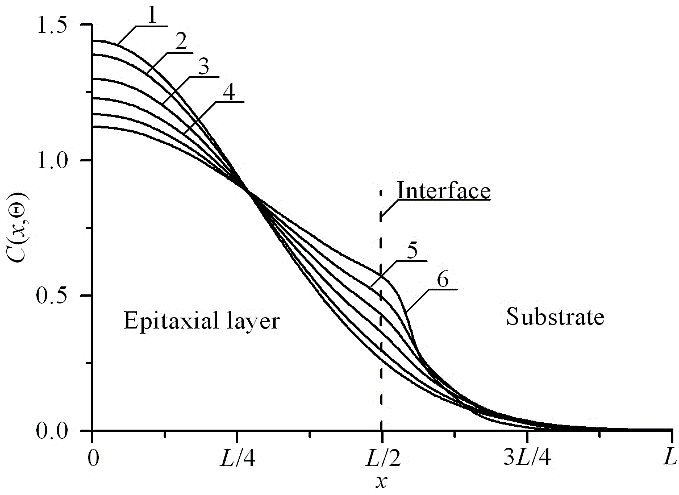
Difference between values of dopant diffusion coefficient in layers of heterostructure increases with increasing of number of curves. Value of dopant diffusion coefficient in the epitaxial layer is larger, than value of dopant diffusion coefficient in the substrate.
Difference between values of dopant diffusion coefficient in layers of heterostructure increases with increasing of number of curves. Value of dopant diffusion coefficient in the epitaxial layer is larger, than value of dopant diffusion coefficient in the substrate. Curve 1 corresponds to homogenous sample and annealing time = 0.0048 (Lx2+Ly2+Lz2)/D0. Curve 2 corresponds to homogenous sample and annealing time = 0.0057 (Lx2+Ly2+Lz2)/D0. Curves 3 and 4 correspond to heterostructure from Figs. 1; annealing times = 0.0048 (Lx2+Ly2+Lz2)/D0 and = 0.0057 (Lx2 +Ly2+Lz2)/D0, respectively.
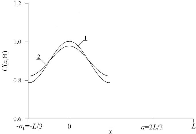
Difference between values of dopant diffusion coefficients increases with increasing of number of curves. Value of dopant diffusion coefficient in this section is smaller, than value of dopant diffusion coefficient in nearest sections.
It should be noted, that framework the considered approach one shall optimize annealing of dopant and/or radiation defects. To do the optimization we used recently introduced criterion [24]–[31]. The optimization based on approximation real distribution by step-wise function (x,y,z) (see Fig. 7 and Fig. 8). Farther the required values of optimal annealing time have been calculated by minimization the following mean- squared error.
(12)
Solid lines are spatial distributions of implanted dopant in system of two epitaxial layers. Dushed lines are spatial distributions of implanted dopant in one epitaxial layer. Annealing time increases with increasing of number of curves.
Increasing of number of curve corresponds to increasing of annealing time.
We show optimal values of annealing time as functions of parameters on Fig. 8 and Fig. 9. It is known, that standard step of manufactured ion-doped structures is annealing of radiation defects. In the ideal case after finishing the annealing dopant achieves interface between layers of heterostructure. If the dopant has no enough time to achieve the interface, it is practicably to anneal the dopant additionally. The Fig. 9 shows the described dependences of optimal values of additional annealing time for the same parameters as for Fig. 8. Necessity to anneal radiation defects leads to smaller values of optimal annealing of implanted dopant in comparison with optimal annealing time of infused dopant.
Increasing of number of curve corresponds to increasing of annealing time.
Curve 1 describes the dependence of the annealing time on the relation a/L and = = 0 for equal to each other values of dopant diffusion coefficient in all parts of heterostructure. Curve 2 describes the dependence of the annealing time on value of parameter for a/L=1/2 and = = 0. Curve 3 describes the dependence of the annealing time on value of parameter for a/L=1/2 and = = 0. Curve 4 describes the dependence of the annealing time on value of parameter for a/L=1/2 and = = 0.
Curve 1 describes the dependence of the annealing time on the relation a/L and = = 0 for equal to each other values of dopant diffusion coefficient in all parts of heterostructure. Curve 2 describes the dependence of the annealing time on value of parameter for a/L=1/2 and = = 0. Curve 3 describes the dependence of the annealing time on value of parameter for a/L=1/2 and = = 0. Curve 4 describes the dependence of the annealing time on value of parameter for a/L=1/2 and = = 0.
4. Conclusions
In this paper we introduce an approach to increase integration rate of bipolar heterotransistors framework single leg N-level cascaded H-bridge multilevel inverter. The approach gives us possibility to decrease area of the elements with smaller increasing of the element’s thickness.
Appendix
Equations for the functions and , i 0, j 0, k 0 and conditions for them
, i1,
, i1, Solutions of the above equations could be written as
where where sn() = sin ( n ); Equations for functions i(x,y,z,t), i 0 to describe concentrations of simplest complexes of radiation defects.
Boundary and initial conditions for the functions takes the form
Solutions of the above equations could be written as
where where sn(x) = sin ( n x/Lx).
Equations for the functions Cij(x,y,z,t) (i 0, j 0), boundary and initial conditions could be written as Functions Cij(x,y,z,t) (i 0, j 0) could be approximated by the following series during solutions of the above equations
Here
References
- [1] Lachin, V. I., & Savelov, N. S. (2001). Electronics Phoenix.
- [2] Alexenko, A. G., & Shagurin, I. I. (1990). Microcircuitry. Radio and communication, moscow, Moscow.
- [3] Avaev, N. A., Naumov, Y. E., & Frolkin, V. T. (1991). Basis of microelectronics.
- [4] Ippolito, C. M., Italia, A., Guerra, R., & Palmisano, G. (2014). Low-power broadband quadrature signal generator based on phase-tunable dividers. Analog integrated circuits and signal processing, 80(3), 459–471. https://doi.org/10.1007/s10470-014-0362-5
- [5] Fathi, D., Forouzandeh, B., & Masoumi, N. (2009). New enhanced noise analysis in active mixers in nanoscale technologies. Nano, 4(4), 233–238. https://doi.org/10.1142/S1793292009001708
- [6] Chachuli, S. A. M., Fasyar, P. N. A., Soin, N., Karim, N. M., & Yusop, N. (2014). Pareto ANOVA analysis for CMOS 0.18 µm two-stage Op-amp. Materials science in semiconductor processing, 24, 9-14. https://doi.org/10.1016/j.mssp.2014.02.035
- [7] Ageev, O. A., Belyaev, A. E., Boltovets, N. S., Ivanov, V. N., Konakova, R. V., Kudryk, Y. Y., … & Sachenko, A. V. (2009). Au-TiBx-n-6H-SiC Schottky barrier diodes: specific features of charge transport in rectifying and nonrectifying contacts. Semiconductors, 43(7), 865–871. https://doi.org/10.1134/S1063782609070070
- [8] Li, Z., Waldron, J., Detchprohm, T., Wetzel, C., Karlicek, R. F., & Chow, T. P. (2013). Monolithic integration of light-emitting diodes and power metal-oxide-semiconductor channel high-electron-mobility transistors for light-emitting power integrated circuits in GaN on sapphire substrate. Applied physics letters, 102(19). https://doi.org/10.1063/1.4807125
- [9] Tsai, J. H., Chiu, S. Y., Lour, W. S., & Guo, D. F. (2009). High-performance InGaP/GaAs pnp δ-doped heterojunction bipolar transistor. Semiconductors, 43, 939–942. https://doi.org/10.1134/S1063782609070227
- [10] Aleksandrov, O. V., Zakhar’in, A. O., Sobolev, N. A., Shek, E. I., Makoviǐchuk, M. I., & Parshin, E. O. (1998). Formation of donor centers upon annealing of dysprosium- and holmium-implanted silicon. Semiconductors, 32(9), 921–923. https://doi.org/10.1134/1.1187515
- [11] Kumar, M. J., & Singh, T. V. (2008). I Quantum confinement effects in strained silicon mosfets. International journal of nanoscience, 7(02n03), 81-84. https://doi.org/10.1142/S0219581X08005195
- [12] Sinsermsuksakul, P., Hartman, K., Bok Kim, S., Heo, J., Sun, L., Hejin Park, H., … & Gordon, R. G. (2013). Enhancing the efficiency of SnS solar cells via band-offset engineering with a zinc oxysulfide buffer layer. Applied physics letters, 102(5). https://doi.org/10.1063/1.4789855
- [13] Reynolds, J. G., Reynolds, C. L., Mohanta, A., Muth, J. F., Rowe, J. E., Everitt, H. O., & Aspnes, D. E. (2013). Shallow acceptor complexes in p-type ZnO. Applied physics letters, 102(15). https://doi.org/10.1063/1.4802753
- [14] Ong, K. K., Pey, K. L., Lee, P. S., Wee, A. T. S., Wang, X. C., & Chong, Y. F. (2006). Dopant distribution in the recrystallization transient at the maximum melt depth induced by laser annealing. Applied physics letters, 89(17). https://doi.org/10.1063/1.2364834
- [15] Bhukya, R., & Kumar, P. S. (2018). Analysis and implementation of unipolar PWM strategies for three phase cascade multilevel inverter fed induction motor drive. International journal of advances in applied sciences, 7(3), 245–254. https://doi.org/10.11591/ijaas.v7.i3.pp245-254
- [16] Şişianu, S. T., Şişianu, T. S., & Railean, S. K. (2002). Shallow p-n junctions formed in silicon using pulsed photon annealing. Semiconductors, 36(5), 581–587. https://doi.org/10.1134/1.1478552
- [17] Bykov, Y. V., Eremeev, A. G., Zharova, N. A., Plotnikov, I. V., Rybakov, K. I., Drozdov, M. N., … & Skupov, V. D. (2003). Diffusion processes in semiconductor structures during microwave annealing. Radiophysics and quantum electronics, 46(8–9), 749–755. https://doi.org/10.1023/B:RAQE.0000025008.97954.1c
- [18] Pankratov, E. L., & Bulaeva, E. A. (2013). Doping of materials during manufacture p–n-junctions and bipolar transistors. Analytical approaches to model technological approaches and ways of optimization of distributions of dopants. Reviews in theoretical science, 1(1), 58–82. https://doi.org/10.1166/rits.2013.1004
- [19] Kozlivsky, V. V. (2003). Modification of semiconductors by proton beams (St. Petersburg: Nauka, 2003) 268 p.
- [20] Gotra, Z. Y. (1991). Technology of microelectronic devices. Radio and communication, Moscow
- [21] Vinetskiy, V. L., & Kholodar, G. A. (1979). Radiative physics of semiconductors. Kiev: naukova dumka.
- [22] Tikhonov, A. N., & Samarskii, A. A. (2005). Equations of mathematical physics (dover books on physics). Dover Publications; Reprint edition. https://www.amazon.com/Equations-Mathematical-Physics-Dover-Books/dp/0486664228
- [23] Carslaw, H. S., & Jaeger, J. C. (1959). Conduction of heat in solids. London: Oxford Univ. Press. https://global.oup.com/academic/product/conduction-of-heat-in-solids-9780198533689?cc=us&lang=en&
- [24] Pankratov, E. L. (2007). Russian Microelectronics. Russian microelectronics, 36(1), 33–39.
- [25] Pankratov, E. L. (2008). Redistribution of a dopant during annealing of radiation defects in a multilayer structure by laser scans for production of an implanted-junction rectifier. International Journal of Nanoscience, 7(04n05), 187-197. https://doi.org/10.1142/S0219581X08005328
- [26] Pankratov, E. L. (2017). On approach to optimize manufacturing of bipolar heterotransistors framework circuit of an operational amplifier to increase their integration rate. Influence mismatch-induced stress. Journal of computational and theoretical nanoscience, 14(10), 4885–4899. https://doi.org/10.1166/jctn.2017.6899
- [27] Pankratov, E. L. (2017). On optimization of manufacturing of two-phase logic circuit based on heterostructures to increase density of their elements. Influence of miss-match induced stress. Advanced science, engineering and medicine, 9(9), 787–801. https://doi.org/10.1166/asem.2017.2043
- [28] Pankratov, E. L., & Bulaeva, E. A. (2015). An approach to increase the integration rate of planar drift heterobipolar transistors. Materials science in semiconductor processing, 34, 260–268. https://doi.org/10.1016/j.mssp.2015.02.054
- [29] Pankratov, E. L. (2017). Multidiscipline modeling in materials and structures. Multidiscipline modeling in materials and structures, 13(4), 664–677. https://www.emerald.com/insight/publication/issn/1573-6105/vol/13/iss/4
- [30] Pankratov, E. L. (2018). On influence of mismatch-induced stress and porosity of materials on manufacturing hetrostructure-based devices. Journal of coupled systems and multiscale dynamics, 6(1), 36–
- [52] https://doi.org/10.1166/jcsmd.2018.1146
- [31] Pankratov, E. L. (2018). On modelling of manufacturing of a high-voltage current driver framework a heterostructures under influence of miss-match induced stress and porosity of materials. Journal of computational and theoretical nanoscience, 15(6–7), 1898–1914. https://doi.org/10.1166/jctn.2018.7329